Inspirasi 12 Pcb Design Rules Simple Dan Minimalis
Poin pembahasan Inspirasi 12 Pcb Design Rules Simple Dan Minimalis adalah :
Inspirasi 12 Pcb Design Rules Simple Dan Minimalis. Dalam dunia skema pcb mungkin Anda pernah mendengar dengan yang namanya kumpulan skema pcb. Komponen dasar skema pcb beserta fungsi dan simbolnya yang harus kamu ketahui, Simak ulasan terkait skema pcb dengan artikel Inspirasi 12 Pcb Design Rules Simple Dan Minimalis berikut ini

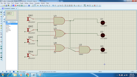
Running Design Rules Check in Cadence PCB Editor Sumber : esdresources.blogspot.com

17 PCB design part IV design rules check YouTube Sumber : www.youtube.com

Pcb design guidelines Sumber : www.slideshare.net

PCB Prototype Fabrication Manufacturer PCB Prototype in Sumber : www.shenzhen2u.com

PCB Design Rules Reference Online Documentation for Sumber : documentation.circuitstudio.com

PCB Information Sumber : pcbinfo.blogspot.com

PCB Design Rules Build Electronic Circuits Sumber : www.build-electronic-circuits.com

PCB Design Rules Build Electronic Circuits Sumber : www.build-electronic-circuits.com

Miniaturization Using Low cost PCB Technology Sumber : www.designworldonline.com

PCB Design Guidelines Eurocircuits PCB Design Guidelines Sumber : www.eurocircuits.com

PCB design guidelines Eurocircuits Sumber : www.eurocircuits.com

Watch videos FEDEVEL Academy Part 2 Sumber : www.fedevel.com

KiCAD design rules Eurocircuits Sumber : www.eurocircuits.com

PCB Design Guidelines Eurocircuits Sumber : www.eurocircuits.com

Rigid Flex Circuit Board Gerber Layout Guidelines Webinar Sumber : www.youtube.com
1Adopt DIY approach in making schematic. ..., 2Properly space the components. ..., 3Do not place traces at right angle. ..., 4Ensure same orientation while placing components. ..., 5Use different wiring directions between two consecutive layers. ..., 6Select the line width for facilitating easy current flow. ..., 7Creating ground plane., 1STEP 1: Take a printout of circuit board layout. ..., 2STEP 2: Cut the Copper Plate for the Circuit Board. ..., 3STEP 3: Transfer the PCB Print onto the Copper Plate., 4STEP 4: Iron the Circuit from the Paper onto the PCB Plate.,
Inspirasi 12 Pcb Design Rules Simple Dan Minimalis. Dalam dunia skema pcb mungkin Anda pernah mendengar dengan yang namanya kumpulan skema pcb. Komponen dasar skema pcb beserta fungsi dan simbolnya yang harus kamu ketahui, Simak ulasan terkait skema pcb dengan artikel Inspirasi 12 Pcb Design Rules Simple Dan Minimalis berikut ini
Running Design Rules Check in Cadence PCB Editor Sumber : esdresources.blogspot.com
Design Rule Check PCB Prototype the Easy Way PCBWay
1 ABSTRACT General layout guidelines for printed circuit boards PCB which exist in relatively obscure documents are summarized Some guidelines apply specifically to microcontrollers however the guidelines are intended to be general and apply to virtually a ll
17 PCB design part IV design rules check YouTube Sumber : www.youtube.com
PCB Design Rules Build Electronic Circuits
24 09 2020 Here you can either specify the rules by hand which is a little bit cumbersome or you can load a design rule file by clicking the Load button Many manufacturers has a pcb design rules file for Eagle ready to be downloaded so that you only need to load it
Pcb design guidelines Sumber : www.slideshare.net
PCB Design Layout Guidelines Hints Tips Electronics
The Basic Design Process The ideal PCB design starts with the discovery that a PCB is needed and continues through the final production boards Fig 1 After determining why the PCB is needed
PCB Prototype Fabrication Manufacturer PCB Prototype in Sumber : www.shenzhen2u.com
13 Basic Rules Of PCB Layout RayPCB com
PCB Design Rules Reference Online Documentation for Sumber : documentation.circuitstudio.com
Top PCB Design Guidelines for PCB Designers PCB Design
Eurocircuits PCB Design Guidelines have been created to help design engineers create PCB layouts that are Right first Time for Manufacture

PCB Information Sumber : pcbinfo.blogspot.com
PCB Design Guidelines For Reduced EMI
A pad is easier to short use one with greater spacing when hand soldered instead Like 10 10 rules is much more easier to solder if you have such spacing in your designed board PCB Thickness The 63 mil PCB thickness appears often as the thickness specification for PCBs
PCB Design Rules Build Electronic Circuits Sumber : www.build-electronic-circuits.com
Basic PCB Design Rules You Should Know Seeed Studio Blog
PCB Design Rules Build Electronic Circuits Sumber : www.build-electronic-circuits.com
The Engineer s Guide To High Quality PCB Design
13 Basic Rules Of PCB Layout 1 According to the circuit module layout the relevant circuit for realizing the same function is called one module and the components in the circuit module should adopt the principle of near concentration the digital circuit and the analog circuit are separated at the same time
Miniaturization Using Low cost PCB Technology Sumber : www.designworldonline.com
PCB Design Guidelines Eurocircuits Eurocircuits PCB
Design rule checking or check s DRC is the area of electronic design automation that determines whether the physical layout of a particular chip layout satisfies a series of recommended parameters called design rules Design rule checking is a major step during physical verification signoff on the design which also involves LVS layout
PCB Design Guidelines Eurocircuits PCB Design Guidelines Sumber : www.eurocircuits.com
PCB design guidelines Eurocircuits Sumber : www.eurocircuits.com
Watch videos FEDEVEL Academy Part 2 Sumber : www.fedevel.com
KiCAD design rules Eurocircuits Sumber : www.eurocircuits.com
PCB Design Guidelines Eurocircuits Sumber : www.eurocircuits.com
Rigid Flex Circuit Board Gerber Layout Guidelines Webinar Sumber : www.youtube.com


0 Comments